|
Visible
rare-earth-doped laser is fabricated on silicon
Much research on photonic devices for
light-based silicon (Si) integrated circuits centers on the 1.5-µm
telecommunications wavelength region; this past year, the advent of Si
lasers and high-speed modulators has been the result (see p. 105). But
another approach-the integration of non-Si semiconductors onto Si
substrates-promises a wider range of wavelengths for many practical uses,
including some beyond the optical transport of information. A group at the
University of Cincinnati Nanoelectronics Laboratory (Nanolab; Cincinnati,
OH) has developed the first of what will likely be a family of rare-earth
(RE)-doped gallium nitride (GaN) coherent light emitters, most of which
lase in the very important visible spectrum.1 The lasers are
fabricated on Si and are potentially compatible with Si CMOS fabrication
techniques. (The Nanolab group has also fabricated similar lasers from
doped GaN grown on sapphire substrates.2)
|
 |
|
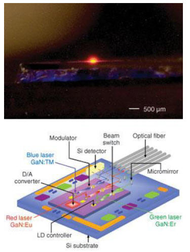
A laser
consisting of europium-doped GaN on a silicon substrate emits at 620
nm (top). The technology potentially allows lasers in the visible,
UV, and IR to be integrated with modulators, photodetectors, and
other photonic components on silicon (bottom). |
The first device consists of an active
0.5-µm-thick GaN planar-waveguide layer doped with 1% europium (Eu) that
is clad with a layer of aluminum gallium nitride (AlGaN). These layers
were deposited onto a (111) Si substrate that already held several layers
of GaN and AlGaN as a buffer, strain reliever, and bottom cladding. The
substrate and layers were then cut and the ends polished to form a
350-µm-long planar laser cavity.
When the Nanolab researchers optically
pumped the laser with 337-nm light from a pulsed nitrogen laser, they
observed gain that saturated at about 95 cm-1 for an 8-MW/cm2
pump intensity; the pump threshold was determined to be 117 kW/cm2.
The emission was polarized, with a spectrum that peaked at 620 nm and
revealed several longitudinal modes spaced apart by 0.4 nm; each mode had
a linewidth (full width at half maximum) of 0.2 nm.
The next step is to make a channel
waveguide cavity, says Andrew Steckl, one of the researchers. We have
obtained preliminary results that indicate that significant increases in
gain will result. The real challenge, notes Steckl, is to electrically
pump the device. We hope to be able to inject sufficient charge density
in a p-i-n structure to generate the necessary density of excited
rare-earth ions for stimulated emission, he says.
One of the attractive features of the
Nanolab approach, notes Steckl, is that there are so many colors available
with various rare earths. Other rare-earth dopants besides europium
include thulium, which emits in the blue (477 nm); erbium, which produces
green (537 to 559 nm) and IR (1.5 µm); gadolinium, which emits in the UV
(300 nm; gadolinium would require an AlGaN host); and others.
The growth process for the doped GaN-on-Si
lasers is CMOS-compatible, says Steckl; the fabrication temperatures are
relatively low (700°C to 800°C) and can be pushed lower with additional
investigation. Our vision is that you could integrate multiple sources on
a single Si chip and control the output with built-in Si electronics, he
says. Such a device could include modulators, photodetectors, and light
routers (see figure).
Steckl sees many potential applications of
the rare-earth-doped GaN-on-Si technology, including displays (very pure
red, green, and blue colors can be emitted); computing (optical
interconnects for increasing the communication speed of chip-to-chip,
processor to peripherals, and so on); low-cost on-chip spectroscopy; and
low-cost discrete laser sources with a rainbow of colors (can combine
rare-earth dopants in one device and generate a variety of colors).
John Wallace
REFERENCES
1. J.H. Park and A.J. Steckl, J. Applied
Physics 98, 056108 (2005).
2. J.H. Park and A.J. Steckl, Appl. Phys.
Lett. 85(20) (Nov. 15, 2005).
|