|
Scanning Electron Microscopy (SEM) and Atomic Force Microscopy
(AFM) are new techniques that
reveal three-dimensional pictures of surfaces with such high resolution
that individual atoms can be imaged. The SEM (pictured bottom left)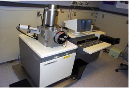 accomplishes this by scanning a conducting probe over
the surface while adjusting the height above the sample to maintain a
constant tunneling current across a very narrow gap. Since the tunneling
current depends exponentially on the gap width, a feedback system can be
used to maintain a gap width to within a fraction of one angstrom. The
lateral resolution of the SEM also results from this strong dependence
of current on
accomplishes this by scanning a conducting probe over
the surface while adjusting the height above the sample to maintain a
constant tunneling current across a very narrow gap. Since the tunneling
current depends exponentially on the gap width, a feedback system can be
used to maintain a gap width to within a fraction of one angstrom. The
lateral resolution of the SEM also results from this strong dependence
of current on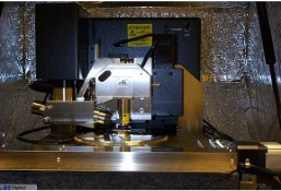 gap distance. There is usually one atom on the
probe that is closer to the substrate than any other, and thus the
tunneling current flows through this one atom. This highly concentrated
current allows the difference in height between the top of the atom on
the substrate and the valleys to the adjacent atoms to be distinguished. With
appropriate computer control, a 3-D image of the surface can be
generated. The AFM determines the contours of a sample surface by using
a cantilever spring to sense the force between the outermost atom on the
probe and the sample surface. We currently use a Digital Instruments
Dimension 3100 atomic force microscope AFM (pictured top right gap distance. There is usually one atom on the
probe that is closer to the substrate than any other, and thus the
tunneling current flows through this one atom. This highly concentrated
current allows the difference in height between the top of the atom on
the substrate and the valleys to the adjacent atoms to be distinguished. With
appropriate computer control, a 3-D image of the surface can be
generated. The AFM determines the contours of a sample surface by using
a cantilever spring to sense the force between the outermost atom on the
probe and the sample surface. We currently use a Digital Instruments
Dimension 3100 atomic force microscope AFM (pictured top right
|