|
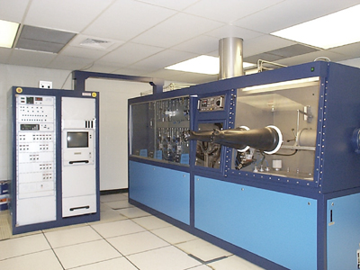
Metalorganic Chemical Vapor Deposition (MOCVD) system in NanoLab is a newly upgraded system for thin film growth. MOCVD technique has been widely employed in semiconductor industry for various thin film growth, which is one of the most critical steps in high technical microfabrications. Our MOCVD system is capable to grow GaN based materials. NH3 is used as N source. Ga, Al and In sources are available for GaN based alloy thin films growth. Eu, Er are the RE elements used for doping by MOCVD. CP2Mg and SiH4 are used for p-type and n-type GaN films growth, respectively. Using IR lampl to heat a graphite susceptor a growth temperature of 1025°C can be reached. A modified safety control system allows the growth performing under both H2 and N2 atmosphere. A glove box with purified N2 circulation gives a perfect separation of the deposition chamber from air. Acid based scrubber ensures that the exhaust gases is cleaned before into air. H2 detection system and NH3 detection system are employed to monitor the MOCVD system for safety purpose. Main properties of the MOCVD system: Sources: - MO: TMGa, TMAl, TMIn - N: NH3 - Doping: Er(thd)3, Eu(thd)3; CP2Mg; SiH4 Growth Temperature: - 950 - 1025°C Heater: - IR lamps Carrier Gases: - H2 or N2 Wafer size: - 2" wafer
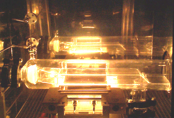
Overview of NanoLab AIX200 MOCVD System (above) Reactor during GaN:RE film growth (down)
|