|
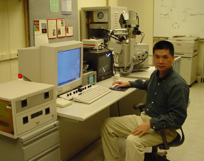
FIB 200 TEM system of FEI Company
provides better performance on overall operations of fabrication of
micro optical devices by Ga+ ion beam micromachining. This system is an advanced tool for rapid, precise
micromachining and deposition of submicron features in various
substrates and materials. It
is also a superb general purpose tool for SEM/TEM specimen cross section
preparation, high contrast imaging, grain structure analysis, high
aspect ratio probe drilling, fabrication of MEMS structures, and other
related applications. The
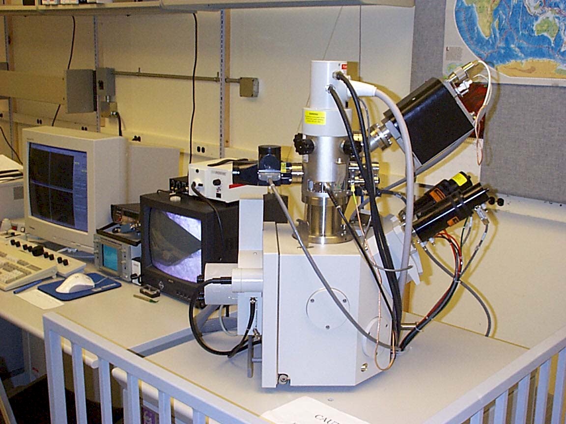
major system specifications include that its accelerating energy range
between 5 - 30 keV. Beam current range from 1 pA - 20 nA for 12
apertures. Beam diameter is 6 - 500 nm. Secondary electron image
resolution is 7 nm. Stage movement accuracy is 0.5 mm.
Maximum stage movement is up to 15 mm. Primary
ion species are Ga and In. It can handle up to 3 inches wafer. Two gas
injection systems are equipped. I2
is used for enhanced etch and XeF2 for insulator enhanced
etch. Other functions include an in-situ optical microscope, real time
milling monitor, auto FIB programmable milling, and selective etch.
|
 Focused
ion beam (FIB) provides strong capability and tremendous flexibility of
nano-fabrication. Based on physical reaction, FIB milling can be applied
to majority of materials.
Focused
ion beam (FIB) provides strong capability and tremendous flexibility of
nano-fabrication. Based on physical reaction, FIB milling can be applied
to majority of materials.