|
An
increasing demand for micro-sensors that can operate at temperature well
above 300°C and often in severe environments (such as those in
automotive and aerospace applications, in combustion processes or gas
turbine control, and in oil industry) has stimulated the search for
alternatives to conventional Si. The research in direct formation of SiC
films on insulating substrates (SiCOI structures) in this study finds a
very promising technology for producing complicated SiC device
structures and provides an excellent alternative material solution for
robust MEMS devices operating at high temperature.
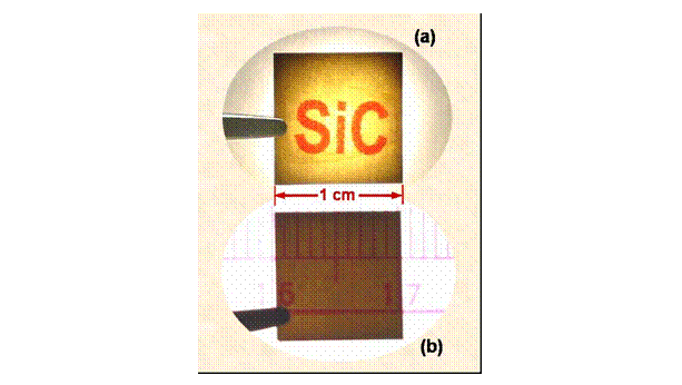
Two
kinds of SiCOI structures, SiC/poly-Si/SiC/Si3N4/Si
for bent-beam strain sensors and SiC/sapphire for electrically passive
fiber-optic temperature sensors, have been fabricated, as shown in the
attached pictures. The research work in this study extends from SiC
thin-film growth using a single organosaline (3MS) precursor and a rapid
thermal LPCVD system, photolithography and ICP etch of SiC thin-films,
as well as material & device characterization. The techniques used to
characterize the as-grown and patterned SiC thin-films and starting
substrates include XRD, SEM, AFM, Hall Effect, four-point probe, mercury
probe, FTIR, XPS, depth profilometer, UV-Visible-IR
absorption/transmission/reflection spectroscopy, and UV-Visible-NIR
fiber.
The ease
of deposition and the ability to deposit large area SiC thin-films on
many different insulating substrates make the SiCOI structures very
attractive for many MEMS applications, particularly in connection with
surface micro-machining fabrication techniques. The growth temperature
and 3MS flow rate are the two key parameters on the grain size and the
distribution of grain orientations, which determine the structural,
electrical and optical properties of the SiC thin-films and related
device performance. Moreover, the ability to use electrically passive
poly-SiC fiber-optic temperature sensors gives the unique advantages of
SiCOI for low-cost, robust, high-temperature applications in harsh
environments. 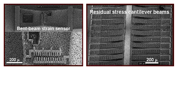 |
 analysis
techniques. Additionally, electrical properties of the SiC films are
mainly measured by Hall effect. At this time, the clear object of
SiC research is trying to optimize growth process to obtain SiC films
with best electrical properties for next generation electronic devices.
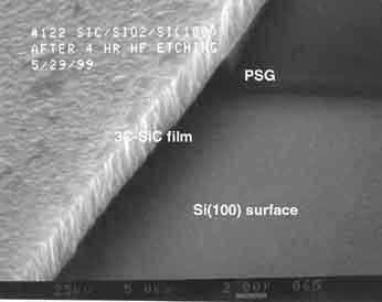
Recently, we have directly grown 3C-SiC(111) on SiO2, Si3N4
and ploy-Si surface by CVD from organosilanes (pictured left), which
makes SiC a perfect material for high temperature MEMS application. In
addition to MEMS application, SiC could also be integrated into the
current Si-based microelectronics fabrication process for gate dieletric
materials and diffusion barrier for Cu interlayers. Finally, this
process could also be used to fabricate SiC SOI structure
analysis
techniques. Additionally, electrical properties of the SiC films are
mainly measured by Hall effect. At this time, the clear object of
SiC research is trying to optimize growth process to obtain SiC films
with best electrical properties for next generation electronic devices.
Recently, we have directly grown 3C-SiC(111) on SiO2, Si3N4
and ploy-Si surface by CVD from organosilanes (pictured left), which
makes SiC a perfect material for high temperature MEMS application. In
addition to MEMS application, SiC could also be integrated into the
current Si-based microelectronics fabrication process for gate dieletric
materials and diffusion barrier for Cu interlayers. Finally, this
process could also be used to fabricate SiC SOI structure