| |
Development of the Rare Earth-doped GaN Material System |
|
Activities include thin film
growth by MBE, surface studies, metallization, doping, etching, and
device characterization. Rare-earth- (RE)-based electroluminescence (EL)
in a matrix of ZnS (or other II-VI compounds) has been the key
ingredient in many display technologies such as electroluminescent
devices (ELDs). Recently, significant progress has been made using the
wide band-gap III-V semiconductor GaN as the host for rare-earth based
photoemission at visible and infrared (IR) wavelengths. In the
past two years it has been shown that RE-doped GaN ELDs can produce
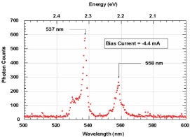
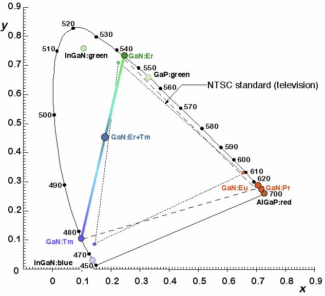
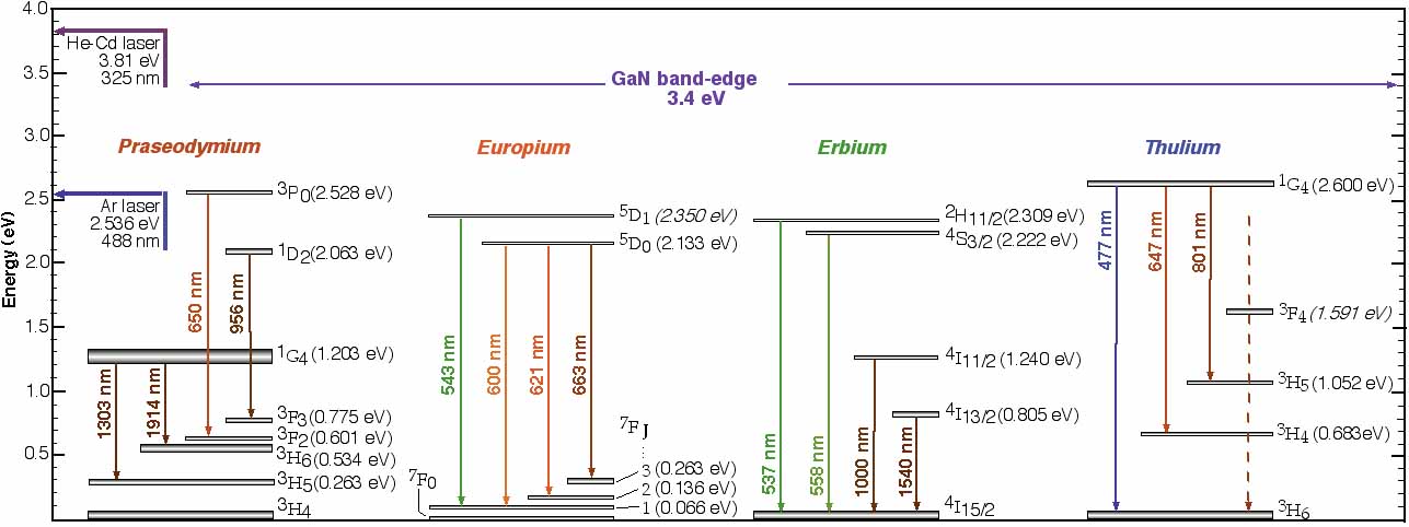
green (based on Er doping), red , (Pr, Eu) and blue light (Tm), as well
as 1.55 µm infrared , emission (Er). The Nanolab utilized molecular
beam epitaxy (MBE) in order to demonstrate the first observation of
visible light emission from GaN:RE. GaN:RE ELDs hold several
promising qualities which are attractive for small- and mid-scale
display and lighting. The emission from a GaN:RE ELD is spectrally sharp
and requires no color filtering since it arises from atomic RE
transitions. The red, green and blue GaN:RE ELDs utilize similiar device
structure and power requirements which could simplify some critical
electrical and material obstacles in multi-color integration of single
color devices. GaN is an advantageous host for RE-based ELDs for several
reasons: it has excellent high field (break down field ~3 MV/cm) carrier
transport can provide hot carriers for impact excitation of the RE ions;
it is transparent to visible RE emission; it is thermally and chemically
rugged; unlike REs in most II-VI hosts the majority of the REs dopant
sits substitutionally on the Ga sublattice preventing some doping
defects due to charge neutrality. Fabrication of the GaN:RE ELDs is a
relatively simple process in terms of the few processing steps involved.
With the present device structures, single ELDs have been operated at
power densities on the order of several hundred W/cm2 in a stable manner
without the usage of a heat sink or active cooling. Below, the
observed RE atomic transistions in GaN are pictured. |
 is
pictured to the left. As part of the LED fabrication the NanoLab is
currently growing epitaxial GaN films on Si with the Riber MBE-32 system
in the Nanolab.
is
pictured to the left. As part of the LED fabrication the NanoLab is
currently growing epitaxial GaN films on Si with the Riber MBE-32 system
in the Nanolab.