|
Focused Ion Beam Micromachining of Microgratings on Arbitrary Angled Facets on Optical Materials |
|
|
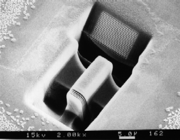
We have invented a technique for micromachining of fine structures on tiny angled facets using a focused ion beam technique. FIB micromachining for the fabrication of optical/photonic devices is an area of expertise at the UC Nanoelectronics Laboratory (NanoLab). The ability to fabricate a diffraction grating of micrometer dimensions on facets of arbitrary angles on an optic chip is very useful for implementing wavelength-division multiplexing (WDM) technology and integrated optics. However, this task is not compatible with conventional fabrication technologies. In the environment of an optical chip, a large number of tiny, precise optical elements are crowded together. Even slight contamination or minor scratching can ruin the entire optical system. However, it is very common to place an optical surface at a certain angle, or to locate an optical element at a specific position. This factor dramatically increases the difficulty of integrated optical system fabrication.
Advantages 1. Using the new technique, a diffractive optical element can be easily integrated into an optoelectronic device such as a WDM demultiplexer, or a tunable semiconductor laser on the same substrate. 2. Gratings created using this technique have pitch sizes from a couple of hundred nanometers to several micrometers, covering the light band from ultraviolet to infrared. 3. The technique eliminates the need for complicated equipment and programming required by traditional diamond ruling and holographic patterning methods. 4. The micrograting fabrication method can be applied to a variety of materials, including any reasonable conductive material (such as semiconductors and metals), and insulators, with the aid of charge neutralizing devices. As a result, the micromachined grating can be integrated naturally into a conventional semiconductor optoelectronic chip. Areas of Application Optoelectronics; fiber optic communications devices; “system-on-a-chip” designs. *For more information, contact the Intellectual Property Office of University of Cincinnati, refer Item Number 102004 |
 Focused
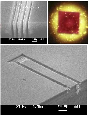
ion beam fabrication and analysis includes milling of GaN bragg gratings
for use in solid state lasers. Most optical devices of GaN-based
materials are grown on sapphire because of good crystal quality.
However, conventional processing procedures are difficult in forming
high reflective laser mirror facets. This difficulty is mainly due
to the large misalignment between sapphire and epitaxial GaN layer.
Currently, laser facets are formed by either the cleaving method or by
dry plasma etching (which generates a large degree of ion-induced
damage). Therefore, the current goal of this project is to look
for a simple and efficient processing technique to fabricate bragg
gratings with low mirror loss and proper mode selection for use in laser
diodes. Pictured to the right is milling experimentation done on
NanoLab GaN. Using the same FIB system but with different goals in
mind, rare earth dopants have been implanted into a variety of hosts.
As an example, praseodymium has been implanted into GaN and bright red
fluorescence obtained that is visible to the naked eye (see top right).
To aid in this leading edge research a liquid metal ion source
fabrication station has been constructed and serves the sole purpose of
allowing creation of a variety of previously researched and novel
implantations sources within the Nanolab.
Focused
ion beam fabrication and analysis includes milling of GaN bragg gratings
for use in solid state lasers. Most optical devices of GaN-based
materials are grown on sapphire because of good crystal quality.
However, conventional processing procedures are difficult in forming
high reflective laser mirror facets. This difficulty is mainly due
to the large misalignment between sapphire and epitaxial GaN layer.
Currently, laser facets are formed by either the cleaving method or by
dry plasma etching (which generates a large degree of ion-induced
damage). Therefore, the current goal of this project is to look
for a simple and efficient processing technique to fabricate bragg
gratings with low mirror loss and proper mode selection for use in laser
diodes. Pictured to the right is milling experimentation done on
NanoLab GaN. Using the same FIB system but with different goals in
mind, rare earth dopants have been implanted into a variety of hosts.
As an example, praseodymium has been implanted into GaN and bright red
fluorescence obtained that is visible to the naked eye (see top right).
To aid in this leading edge research a liquid metal ion source
fabrication station has been constructed and serves the sole purpose of
allowing creation of a variety of previously researched and novel
implantations sources within the Nanolab.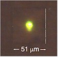 molecular-beam
epitaxy in the Nanolab, hydride vapor-phase epitaxy, and metalorganic
chemical-vapor deposition. After implantation, the GaN samples were
annealed at 1100° C for 1h in various
ambients (Ar, N2, and O2). Strong green
upconversion was observed at 523nm and 546nm under red (840nm) and
infrared (1.0m m) excitation. Upconversion
intensity was measured for Er doses ranging from 4.3´
1012 to 2.4´ 1016
atoms/cm2. Maximum upconversion intensity at 546nm was
observed at a dose of 1~2´ 1015
atoms/cm2, which corresponds to an atomic percentage of
0.3~0.6%. Upconversion is pictured to the left, with the laser
spot size defining the region of emission within the rectangular implant
reg
molecular-beam
epitaxy in the Nanolab, hydride vapor-phase epitaxy, and metalorganic
chemical-vapor deposition. After implantation, the GaN samples were
annealed at 1100° C for 1h in various
ambients (Ar, N2, and O2). Strong green
upconversion was observed at 523nm and 546nm under red (840nm) and
infrared (1.0m m) excitation. Upconversion
intensity was measured for Er doses ranging from 4.3´
1012 to 2.4´ 1016
atoms/cm2. Maximum upconversion intensity at 546nm was
observed at a dose of 1~2´ 1015
atoms/cm2, which corresponds to an atomic percentage of
0.3~0.6%. Upconversion is pictured to the left, with the laser
spot size defining the region of emission within the rectangular implant
reg