|
Black thick dielectric ac
electroluminescence devices (BDEL) utilizing GaN doped with rare earths
(Er-green, Eu-red, Tm-blue) 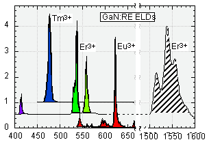 have
been developed at the University of Cincinnati Nano-Electronics
Laboratory for flat panel device applications. The BDEL device structure
operates by applying an ac voltage that is capacitivly coupled to a
phosphor which emits light during reversible electrical breakdown. The
rare earths are excited by hot electron impact excitation during GaN:RE
phosphor break down. Thus, the sharp line admissions of the rare earths
doped into the wide band gap GaN host (3.4 eV) form an ideal durable
material for flat panel display applications. In the BDEL fabrication
process: (1) patterned Indium Tin Oxide (ITO) column electrodes have
been developed at the University of Cincinnati Nano-Electronics
Laboratory for flat panel device applications. The BDEL device structure
operates by applying an ac voltage that is capacitivly coupled to a
phosphor which emits light during reversible electrical breakdown. The
rare earths are excited by hot electron impact excitation during GaN:RE
phosphor break down. Thus, the sharp line admissions of the rare earths
doped into the wide band gap GaN host (3.4 eV) form an ideal durable
material for flat panel display applications. In the BDEL fabrication
process: (1) patterned Indium Tin Oxide (ITO) column electrodes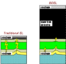 are sputtered onto the viewing glass, (2) a thin dielectric is
sputtered, (3) the GaN:RE
phosphor is deposited by Molecular Beam Deposition (MBD), (4) a thin
dielectric is sputtered, the thick black dielectric is printed, and (5)
patterned Al row electrodes are sputtered. The MBD system, from SVT
Associates, is similar to MBE
except with base pressures at 10-9 and the absence of a
substrate lattice necessary for
epitaxial growth. Unlike Shotcky diode electroluminescence devices (dc-ELD),
traditional thin film electroluminescence devices (TFEL), and Organic
Light Emitting Displays (OLED),
the thick film provides protection against shorts caused by small
fabrication defects (fig 2). This enables fabrication with less costly facilities and
greater dependability. Unlike the inverted thick dielectric
electroluminescence devices (iTDEL) the BDEL devices are fabricated
using the viewing glass as the
are sputtered onto the viewing glass, (2) a thin dielectric is
sputtered, (3) the GaN:RE
phosphor is deposited by Molecular Beam Deposition (MBD), (4) a thin
dielectric is sputtered, the thick black dielectric is printed, and (5)
patterned Al row electrodes are sputtered. The MBD system, from SVT
Associates, is similar to MBE
except with base pressures at 10-9 and the absence of a
substrate lattice necessary for
epitaxial growth. Unlike Shotcky diode electroluminescence devices (dc-ELD),
traditional thin film electroluminescence devices (TFEL), and Organic
Light Emitting Displays (OLED),
the thick film provides protection against shorts caused by small
fabrication defects (fig 2). This enables fabrication with less costly facilities and
greater dependability. Unlike the inverted thick dielectric
electroluminescence devices (iTDEL) the BDEL devices are fabricated
using the viewing glass as the 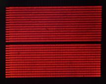 substrate. This avoids the high cost associated with ceramic substrates
and eliminates the need for additional planarization fabrication steps necessary to smooth the rough ceramic surface.
In less than two years of development
this technology has experienced
growth from fabrication of simple 3 mm test device dots to a 40 x 30
matrix addressed monochrome
display utilizing GaN:Eu as the active phosphor. This technology is
presently being developed with collaboration from Extreme Photonix LLC.
Further information can be obtained from previous publications in IEEE
and the SID digest. substrate. This avoids the high cost associated with ceramic substrates
and eliminates the need for additional planarization fabrication steps necessary to smooth the rough ceramic surface.
In less than two years of development
this technology has experienced
growth from fabrication of simple 3 mm test device dots to a 40 x 30
matrix addressed monochrome
display utilizing GaN:Eu as the active phosphor. This technology is
presently being developed with collaboration from Extreme Photonix LLC.
Further information can be obtained from previous publications in IEEE
and the SID digest. |